Search
Pin Diode Switches - DPDTFrom 100 MHz to 24 GHz, any optimized bandwidth is available in absorptive or reflective models. Units can be customized for your application with offerings of various isolations, switching speeds, size configurations and even matched phase and amplitude. Control options include solder pins, SMA or SMC Connector, and Multi-Pin connector. |
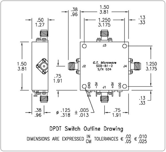 |
Frequency Ranges: From 100 MHz to 24 GHz, any optimized bandwidth is available.
TTL Compatible Logic: Logic ‘1’ = Low Loss J1-J2/J3-J4 and Logic ‘0’ = Low Loss J1-J4/J2-J3. Switches without a TTL driver, +1 VDC @ +60 mA = Low Loss J1-J2 and -1 VDC @ -60 mA = Low Loss J3-J4 on 2 independent logic inputs or vice versa for J1-J4/J2-J3. For additional logic options, please consult the factory.
High Speed Switching: Switches are measured from 50% TTL to 10% / 90% RF from any set value to any set value.
Operating Temperature Range: Standard models include temperature compensation in a range from -55° to +85° C. For more severe environments, please consult the factory.
Low DC Power Consumption: Switches with TTL drivers require ±5 VDC @ ±60 mA.
High RF Power Handling: For power levels greater than listed, please consult the factory.
Standard Interfaces: RF port connectors are ‘SMA’ female per MIL-C-39012. DC/Logic connections are solder terminals. Please consult the factory for additional options.
Matched Phase & Amplitude: Models listed are available with matched ports. Please consult the factory.
Outline Size & Diagram
For substantial improvement in performance, ask for optimized narrowband models.
|
Electrical Specifications for DPDT Transfer Switches |
|||||||||
|
Frequency Range (GHz) |
Isolation (dB) |
Insertion Loss (dB) & Switching Speed |
Insertion Loss (dB) & Switching Speed |
Insertion Loss (dB) & Switching Speed |
VSWR |
Input Power CW/Max (Watts) |
|||
|
Loss |
µSec |
Loss |
ηSec |
Loss |
ηSec |
||||
|
0.5-2.0 |
30 |
0.70 |
1.0 |
0.95 |
100 |
1.00 |
30 |
1.4:1 |
0.1/1.0 |
|
60 |
0.90 |
1.10 |
1.20 |
||||||
|
2.0-8.0 |
30 |
2.00 |
2.00 |
2.25 |
1.6:1 |
0.2/1.0 |
|||
|
60 |
2.50 |
2.50 |
2.75 |
1.8:1 |
|||||
|
6.0-18.0 |
30 |
3.10 |
3.10 |
3.30 |
2.0:1 |
||||
|
60 |
3.40 |
3.40 |
3.60 |
||||||
|
2.0-18.0 |
30 |
3.10 |
3.10 |
3.30 |
|||||
|
60 |
3.40 |
3.40 |
3.60 |
||||||
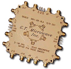
Pin Diode Switches - SP16TFrom 100 MHz to 24 GHz, any optimized bandwidth is available in absorptive or reflective models. These are available in any combination between a SP9T to a SP16T. Units can be customized for your application with offerings of various isolations, switching speeds, size configurations and even matched phase and amplitude. Control options include solder pins or Multi-Pin connector. |
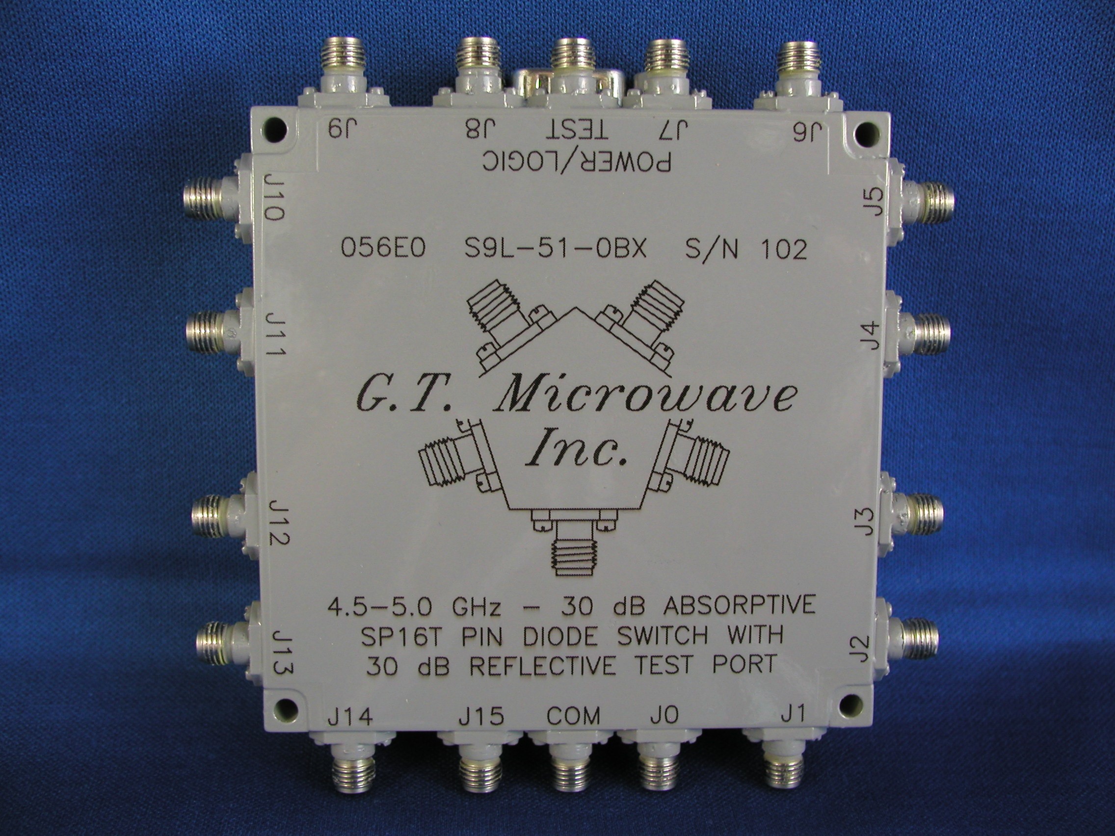 |
Frequency Ranges: From 100 MHz to 20 GHz, any optimized bandwidth is available.
TTL Compatible Logic: The control logic consists of 5 BITs, binary, TTL compatible logic with a two unit load at 0.8 mA.
High Speed Switching: Switch is measured from 50% TTL to 10% / 90% RF from any set value to any set value.
Operating Temperature Range: This model includes temperature compensation in a range from -40° to +70° C. For more severe environments, please consult the factory.
Low DC Power Consumption: Switches with TTL drivers require ±5 VDC @ +850/-200 mA.
High RF Power Handling: For power levels greater than listed, please consult the factory.
Standard Interfaces: RF port connectors are ‘SMA’ female per MIL-C-39012. DC/Logic connections are solder terminals. Please consult the factory for additional options.
Matched Phase & Amplitude: Model listed is matched port-to-port with an amplitude match of ±0.5 dB and a phase match of ±5.0 degrees.
Outline Diagram
For substantial improvement in performance, ask for optimized narrowband models.
|
Electrical Specifications for SP16T Absorptive PIN Diode Switch |
||||||
|
Frequency Range (GHz) |
Isolation (dB) |
Insertion Loss (dB) |
VSWR |
Operational/Survival RF Power (dBm/Watts) |
Switching Speed (µSec) |
Outline Size (inches) |
|
2.0-18.0 |
60 |
7.0 |
2.0:1, On or Off |
+20/1.0 |
2.0 |
3.50 x 3.50 x 0.88 |
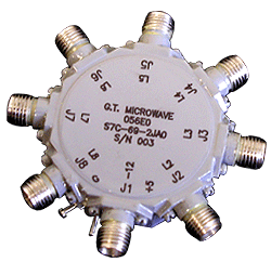
Pin Diode Switches - SP7TFrom 100 MHz to 24 GHz, any optimized bandwidth is available in absorptive or reflective models. Units can be customized for your application with offerings of various isolations, switching speeds, size configurations and even matched phase and amplitude. Control options include solder pins or Multi-Pin connector. These units are available in a rectangular or round configuration |
 |
Frequency Ranges: From 100 MHz to 24 GHz, any optimized bandwidth is available.
TTL Compatible Logic: Logic ‘1’ = Isolation and Logic ‘0’ = Insertion Loss. For switches without a TTL driver, +1 VDC @ +50 mA = Isolation and -1 VDC @ -50 mA = Insertion Loss. For additional logic options, please consult the factory.
High Speed Switching: Switches are measured from 50% TTL to 10% / 90% RF from any set value to any set value.
Operating Temperature Range: Standard models include temperature compensation in a range from -55° to +85° C. For more severe environments, please consult the factory.
Low DC Power Consumption: Switches with TTL drivers require ±5 VDC @ +300/-80 mA.
High RF Power Handling: For power levels greater than listed, please consult the factory.
Absorptive Switches: The J2-J8 ports are non-reflective.
Standard Interfaces: RF port connectors are ‘SMA’ female per MIL-C-39012. DC/Logic connections are solder terminals. Please consult the factory for additional options.
Matched Phase & Amplitude: Models listed are available with matched ports. Otherwise, add 0.25 dB loss to ports J2 & J8. Please consult the factory.
Outline Size & Diagram
For substantial improvement in performance, ask for optimized narrowband models.
|
Electrical Specifications for Reflective & Absorptive SP7T Switches |
||||||||||||
|
Frequency Range (GHz) |
Isolation (dB) |
Insertion Loss (dB) & Switching Speed |
Insertion Loss (dB) & Switching Speed |
Insertion Loss (dB) & Switching Speed |
VSWR |
Input Power Typical/Max (Watts) |
||||||
|
REFL |
ABS |
µSec |
REFL |
ABS |
ηSec |
REFL |
ABS |
ηSec |
||||
|
0.5-2.0 |
30 |
0.70 |
1.10 |
1.0 |
0.90 |
1.30 |
100 |
1.00 |
1.40 |
30 |
1.5:1 |
0.1/1.0 |
|
60 |
0.90 |
1.30 |
1.10 |
1.50 |
1.20 |
1.60 |
||||||
|
80 |
1.00 |
1.40 |
1.20 |
1.60 |
1.30 |
1.70 |
||||||
|
2.0-8.0 |
30 |
2.00 |
2.25 |
2.00 |
2.25 |
2.40 |
2.50 |
1.7:1 |
0.2/1.0 |
|||
|
60 |
2.30 |
2.50 |
2.30 |
2.50 |
2.60 |
2.75 |
||||||
|
80 |
2.30 |
2.50 |
2.30 |
2.50 |
2.60 |
2.75 |
||||||
|
6.0-18.0 |
30 |
3.25 |
3.45 |
3.25 |
3.45 |
2.85 |
3.25 |
2.0:1 |
||||
|
60 |
3.55 |
3.75 |
3.55 |
3.75 |
3.05 |
3.45 |
||||||
|
80 |
3.55 |
3.75 |
3.55 |
3.75 |
3.25 |
3.65 |
||||||
|
2.0-18.0 |
30 |
3.25 |
3.45 |
3.25 |
3.45 |
3.50 |
3.70 |
|||||
|
60 |
3.55 |
3.75 |
3.55 |
3.75 |
3.75 |
3.95 |
||||||
|
80 |
3.75 |
4.50 |
3.75 |
4.50 |
3.75 |
4.50 |
||||||
Pin Diode Switches - SP8TFrom 100 MHz to 24 GHz, any optimized bandwidth is available in absorptive or reflective models. Units can be customized for your application with offerings of various isolations, switching speeds, size configurations and even matched phase and amplitude. Control options include solder pins or Multi-Pin connector. These units are available in a rectangular or round configuration |
 |
Frequency Ranges: From 100 MHz to 24 GHz, any optimized bandwidth is available.
TTL Compatible Logic: Logic ‘1’ = Isolation and Logic ‘0’ = Insertion Loss. For switches without a TTL driver, +1 VDC @ +50 mA = Isolation and -1 VDC @ -50 mA = Insertion Loss. For additional logic options, please consult the factory.
High Speed Switching: Switches are measured from 50% TTL to 10% / 90% RF from any set value to any set value.
Operating Temperature Range: Standard models include temperature compensation in a range from -55° to +85° C. For more severe environments, please consult the factory.
Low DC Power Consumption: Switches with TTL drivers require ±5 VDC @ +350/-85 mA.
High RF Power Handling: For power levels greater than listed, please consult the factory.
Absorptive Switches: The J2-J9 ports are non-reflective.
Standard Interfaces: RF port connectors are ‘SMA’ female per MIL-C-39012. DC/Logic connections are solder terminals. Please consult the factory for additional options.
Matched Phase & Amplitude: Models listed are available with matched ports. Otherwise, add 0.25 dB loss to ports J2 & J9. Please consult the factory.
Outline Size & Diagram
For substantial improvement in performance, ask for optimized narrowband models.
|
Electrical Specifications for Reflective & Absorptive SP8T Switches |
||||||||||||
|
Frequency Range (GHz) |
Isolation (dB) |
Insertion Loss (dB) & Switching Speed |
Insertion Loss (dB) & Switching Speed |
Insertion Loss (dB) & Switching Speed |
VSWR |
Input Power Typical/Max (Watts) |
||||||
|
REFL |
ABS |
µSec |
REFL |
ABS |
ηSec |
REFL |
ABS |
ηSec |
||||
|
0.5-2.0 |
30 |
0.75 |
1.15 |
1.0 |
0.95 |
1.35 |
100 |
1.05 |
1.45 |
30 |
1.5:1 |
0.1/1.0 |
|
60 |
0.95 |
1.35 |
1.15 |
1.55 |
1.25 |
1.65 |
||||||
|
80 |
1.10 |
1.50 |
1.30 |
1.70 |
1.40 |
1.80 |
||||||
|
2.0-8.0 |
30 |
1.20 |
1.60 |
1.40 |
1.80 |
1.50 |
1.90 |
1.7:1 |
0.2/1.0 |
|||
|
60 |
2.20 |
2.50 |
2.20 |
2.50 |
2.40 |
2.70 |
||||||
|
80 |
2.20 |
2.50 |
2.20 |
2.50 |
2.40 |
2.70 |
||||||
|
6.0-18.0 |
30 |
4.00 |
4.25 |
5.25 |
5.25 |
5.00 |
5.25 |
2.0:1 |
||||
|
60 |
4.30 |
4.50 |
5.50 |
5.50 |
5.25 |
5.50 |
||||||
|
80 |
4.30 |
4.50 |
5.50 |
5.50 |
5.25 |
5.50 |
||||||
|
2.0-18.0 |
30 |
4.00 |
4.25 |
5.00 |
5.25 |
5.00 |
5.25 |
|||||
|
60 |
4.30 |
4.60 |
5.25 |
5.50 |
5.25 |
5.50 |
||||||
|
80 |
4.30 |
4.60 |
5.25 |
5.50 |
5.25 |
5.50 |
||||||
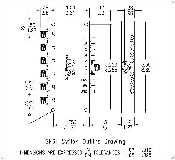
Pin Diode Switches - SP6TFrom 100 MHz to 24 GHz, any optimized bandwidth is available in absorptive or reflective models. Units can be customized for your application with offerings of various isolations, switching speeds, size configurations and even matched phase and amplitude. Control options include solder pins or Multi-Pin connector. These units are available in a rectangular or round configuration |
 |
Frequency Ranges: From 100 MHz to 24 GHz, any optimized bandwidth is available.
TTL Compatible Logic: Logic ‘1’ = Isolation and Logic ‘0’ = Insertion Loss. For switches without a TTL driver, +1 VDC @ +50 mA = Isolation and -1 VDC @ -50 mA = Insertion Loss. For additional logic options, please consult the factory.
High Speed Switching: Switches are measured from 50% TTL to 10% / 90% RF from any set value to any set value.
Operating Temperature Range: Standard models include temperature compensation in a range from -55° to +85° C. For more severe environments, please consult the factory.
Low DC Power Consumption: Switches with TTL drivers require ±5 VDC @ +250/-75 mA.
High RF Power Handling: For power levels greater than listed, please consult the factory.
Absorptive Switches: The J2-J7 ports are non-reflective.
Standard Interfaces: RF port connectors are ‘SMA’ female per MIL-C-39012. DC/Logic connections are solder terminals. Please consult the factory for additional options.
Matched Phase & Amplitude: Models listed are available with matched ports. Otherwise, add 0.25 dB loss to ports J2 & J7. Please consult the factory.
Outline Size & Diagram
For substantial improvement in performance, ask for optimized narrowband models.
|
Electrical Specifications for Reflective & Absorptive SP6T Switches |
||||||||||||
|
Frequency Range (GHz) |
Isolation (dB) |
Insertion Loss (dB) & Switching Speed |
Insertion Loss (dB) & Switching Speed |
Insertion Loss (dB) & Switching Speed |
VSWR |
Input Power Typical/Max (Watts) |
||||||
|
REFL |
ABS |
µSec |
REFL |
ABS |
ηSec |
REFL |
ABS |
ηSec |
||||
|
0.5-2.0 |
30 |
0.65 |
1.05 |
1.0 |
0.85 |
1.25 |
100 |
0.95 |
1.35 |
30 |
1.5:1 |
0.1/1.0 |
|
60 |
0.85 |
1.25 |
1.05 |
1.45 |
1.15 |
1.55 |
||||||
|
80 |
0.95 |
1.35 |
1.15 |
1.55 |
1.25 |
1.65 |
||||||
|
2.0-8.0 |
30 |
1.05 |
1.45 |
1.25 |
1.65 |
1.35 |
1.75 |
1.7:1 |
0.2/1.0 |
|||
|
60 |
1.40 |
1.80 |
1.60 |
2.00 |
1.70 |
2.10 |
||||||
|
80 |
1.50 |
1.90 |
1.70 |
2.10 |
1.80 |
2.20 |
||||||
|
6.0-18.0 |
30 |
3.00 |
3.20 |
2.60 |
3.00 |
3.20 |
3.40 |
2.0:1 |
||||
|
60 |
3.50 |
3.50 |
3.00 |
3.20 |
3.50 |
3.70 |
||||||
|
80 |
3.50 |
3.50 |
3.30 |
3.50 |
3.50 |
3.70 |
||||||
|
2.0-18.0 |
30 |
3.00 |
3.20 |
3.00 |
3.20 |
3.20 |
3.40 |
|||||
|
60 |
3.30 |
3.50 |
3.30 |
3.50 |
3.50 |
3.70 |
||||||
|
80 |
3.30 |
3.50 |
3.30 |
3.50 |
3.50 |
3.70 |
||||||