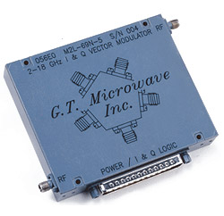
Broadband I & Q Vector Modulator
Demonstrates the Leading Edge in Performance
 |
The function of an I & Q Vector Modulator is to simultaneously control the phase and amplitude characteristics in the processing of a microwave signal. This device will convert a signal to a desired vector location via a digital command. The theory of operation is to divide the input signal into two equal signals 90 degrees apart, I (In-Phase) and Q (Quadrature). This allows the magnitude of each signal to be relocated along its vectors' axis. The two signals are then combined. Using the Pythagorean Theorem, the sum of the vectors produces the resultant output signal. |
The circuit for an I & Q Vector Modulator consists of a 3 dB, 90 degree Quadrature Hybrid, two Variable Attenuators capable of a 180 degree phase shift, an In-Phase Power Combiner and drive circuits to control the Variable Attenuators.
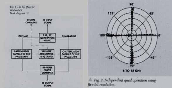
The key component is a 3 dB, 90 degree, Quadrature Hybrid. The hybrid is used nine times in a Vector Modulator. The input signal is processed by the first hybrid. It equally divides the amplitude with a 90 degree phase shift to the quadrature path and the two signals are isolated. This places the I & Q Vectors on their respective axis. The balance of the hybrids are divided in the I & Q channels for the Variable Attenuators. Each attenuator controls the magnitude with 180 degree phase shift allowing four quadrant operation. The final stage is the In-Phase Power Combiner which combines the signals in vector addition to the output.
In the RF design of a Vector Modulator the preferred media is microstrip. Traditional hybrids are designed in stripline. Whether incorporating the hybrid as part of the circuit or as a discrete component like hybrids for microstrip configurations, the result is, the microwave fields of propagation are excited. This creates a discontinuity within the transmission line of the device. Techniques can be employed to minimize the discontinuity; but with nine 4 port hybrids, this event occurs directly or in-directly 36 times. To this end, changing media alters fringing fields, thus creating adverse effects and degrading performance.
In a very natural progression, G. T. Microwave developed hybrids in microstrip to eliminate the 36 discontinuities; this complements the design. In a stripline hybrid, tuning is performed between measurements because the hybrid's circuitry is not accessible. Microstrip
hybrids allow access to the circuitry while being measured. This provides for a more precise tuning capability. The technique yielded an overall improvement in both the optimization and performance. The hybrid exhibits a 4:1 Bandwidth with an Amplitude Balance of +/- 0.5 dB, a Phase Balance of +/- 2 degrees, an Isolation of 25 dB min and a V.S.W.R. of 1.3:1 max.
With the transmission problems eliminated by the entire microwave circuit topology being in a true microstrip configuration, there were other design considerations that were incorporated.
The choice of a diode is an important design consideration. Using chip diodes with a ribbon lead in a shunt configuration has its drawbacks. In a high frequency broadband application, the inductance of ribbon lead adversely effects the attenuation and phase. A Beam
Lead Diode installed using a proprietary technique reduces the series inductance and has a significant improvement in performance.
To minimize adverse effects from biasing, the networks are buried as far as possible from the direct signal paths. The line length between adjacent hybrids is zero in the I & Q channels for optimal broadband performance.
Even with the improvement in the microwave performance, it is the control circuitry that provides the absolute accuracy for the overall device.
The digitally controlled section of the Vector Modulator is designed as two independent drivers, hence I & Q. Each driver has a resolution capable of 64K to control and compensate the device. For any desired control input slope characteristic, the optimal performance values are stored in the driver's EEproms ready to be commanded from the external I and Q Digital Control Input.
This is accomplished by using a computer with I/O and IEEE controller cards, G. T. Microwave's proprietary program and a Vector Network Analyzer. The computer's I/O port sets the external control input for I or Q then ramps each driver's 64K of resolution along the I & Q
Vectors using another I/O port to an internal control input. While ramping the drivers the Vector Network Analyzer measures each step and sends the data to the computer via the IEEE Bus. The optimal performance is mathematically calculated by the computer and the driver's EEproms are programmed for the control input slope.
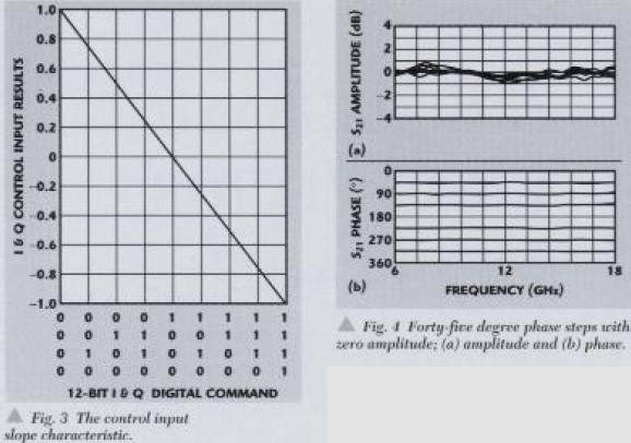
For the control input slope characteristic of the I & Q channels to be linear with voltage
the computer uses the following equations:
Attenuation (dB) = 20 log ((1-(input count/2048)) for input count from 0 to 2048
Attenuation (dB) = 20 log ((input count/2048)-1) for input count from 2049 to 4095
Operating an I & Q Vector Modulator for simultaneous control of attenuation and phase shift is accomplished by finding their respective I and Q as follows:
I = 10-(dB/20) cos 0
Q = 10-(dB/20) sin 0
Where dB = desired attenuation and 0 = desired phase shift.
The I and Q results are submitted to the Control Input Connector as commands:
I digital count = 2048 (1 - I)
Q digital count = 2048 (1-Q)
Example:
Desired output; -3.0 dB of attenuation and 45 degrees of phase shift
I = (.707) (.707) = 0.5
Q = (.707) (.707) = 0.5
Commands to Digital Control Input:
I digital count = 2048 (1 - 0.5) = 1024
Q digital count = 2048 (1 - 0.5) = 1024
The Vector Modulator being demonstrated is optimized over a 3:1 bandwidth, 6.0-18.0 GHz with 20 dB of attenuation and 360 degrees of phase shift and with both I and Q channels at maximum attenuation (input count = 2048) isolation greater than 30 dB. The unit's envelope conformed to form, fit and function of an industry standard packaging. Using two independent test laboratories to verify results, the following test data illustrates the typical performance that is achieved using the techniques described herein (see Figures 3 through 8).
This technology hosts a variety of products which include but is not limited to: BPSK, QPSK & Vector Modulators, Phase Shifters and Phase Free Attenuators. The models are offered with options that include: digital control with up to 64K of resolution, linearized or any desired control input slope characteristic, narrowband optimized performance, temperature compensation, video filtering and sub-assembly integration.